Page Contents
Overview
These notes just scratch the surface of the very deep, interesting, and practical area of switch architecture. We emphasize some key concepts that come up frequently in the design of switches and that have wide applicability across multiple technologies. To start we take a look at how the marketing and sales of commercial switches can get a bit silly.
Building a Switch with Marketing’s Help
Our goal will be to create the highest capacity switch ever built for the lowest cost!
-
For highest capacity we’ll have it work with DWDM signals
-
Assume each fiber has 100 wavelengths each carrying 100Gbps implies 10Tbps per link (Marketing says we can double or triple this based on the wavelength capacity of a fiber).
-
Assume that we can get 100 fiber pairs onto the front panel with careful cable management.
-
We now have a switch with 100 x 10Tbps = 1.0Pbps! The world’s first Peta bit per second capacity switch.
-
-
But how will the switch actually work?
- We’ll have “double” receptacles for each front panel plug.
- When a connection request comes in we’ll page Bob our engineering technician and have him connect a “patch cord” between the fibers.
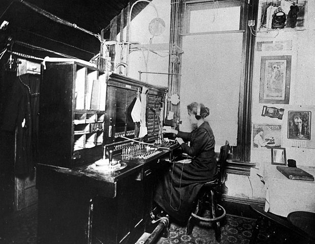
- Hmm, this seems a bit fishy and familiar. Isn’t this just a fiber optic path panel? Sounds like we reinvented an old fashioned telephone switch board. See Figure 1!
-
Do folks see any issues with this?
- Doesn't it seem like this approach would have really slow switching time. No offense to Bob. Hmm, we really need to automate this...
- Any other issues? What's the smallest amount of bandwidth our switch can switch? This is the concept of switching granularity.
Switch Performance Measures
As the previous section showed there is more that just one dimension to switch performance, e.g. raw switching capacity. In general we will be interested in:
-
Throughput: the agregate rates that are switched. Along these lines we have from fastest to slowest:
- Port switching, i.e., like an automated patch panel. Since WDM fibers currently carry the most bits switching between such fibers offers the highest "throughput" switching.
- Wavelength switching as done in wavelength switched optical networks. Each wavelength can transport 10Gbps, 40Gbps, 100Gbps or more.
- Time Division Multiplexed switching channels generally run near the rates of individual wavelength channels.
- Packet Switching. These generally run near the rates of individual TDM or wavelength channels.
-
Granularity: The problem with our previously designed switch was its coarse granularity (10 Tera bit per second). Few users can directly deal with flows such as this. Hence finer granularity is generally desired and can result in less bandwidth being "wasted" or "stranded". Note that the finer granularity switching is currently done electronically rather than optically. From finest to coarsest we have:
- Packet switching can switch just one packet between a source and destination, there is no minimum granularity imposed by the technology.
- TDM: Older TDM technology included 64kbps channels to accomodate voice. However most voice traffic is being moved over to packet networks. Some private line services still use 1.5Mbps (T1) or 2 Mbps (E1) channels, but most TDM services are based on either 50Mbps or 2.5Gbps granularity.
- Wavelength switching: most wavelengths today are used for 10Gbps or higher signals resulting in fairly coarse granularity.
- Port switching
-
Cost & Power per bit (from least expensive to most expensive)
- Port switching (optical)
- Wavelength switching
- TDM switching
- Packet switching
-
Time to Switch: Some devices particularly optical technologies can have fairly long times to transition from one switching configuration to another. Faster changes are better. In general we have from fastest to slowest:
- Packet switching
- TDM switching
- Optical switching (wavelength or ports)
General Structure of Switches
Telecommunications and data communications switches come in a wide variety of shapes and sizes, and are implemented in a wide variety of ways. We'll highlight the general structure of a switch here. In general we can decompose a switch into the following parts as shown in Figure 2.
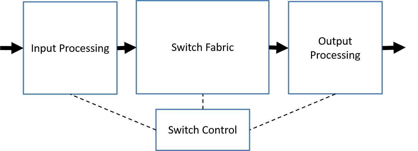
- Input processing
- Optical/Wavelength switching: may include optical amplification or automatic gain control (to keep signal levels within the range of the switch fabric)
- TDM: may contain optical to electrical conversion, framing, link related OA&M, processing of overhead bytes, serial to parallel conversion.
- Packet switching: may contain optical to electrical conversion, serial to parallel conversion, physical and link layer processing, input packet processing (we'll discuss this more later)
- Output processing
- Optical/Wavelength switching: may include: wavelength combining, optical amplification,
- TDM: may include: parallel to serial conversion and framing, electrical to optical conversion.
- Packet switching: output packet processing (including queueing), link and physical layer processing, may include: parallel to serial conversion, electrical to optical conversion. We'll be studying more on output processing when we look at Quality of Service (QoS) in packet networks.
- Switching Fabric
- Responsible for "transporting" signals, TDM frames, or packets (or parts of packets) between input processing and output processing sections. We'll be studying commonly used techniques to create switch fabrics in these lectures.
- Switch Control: Coordinates input processing, output processing, and the switch fabric to produce the desired switching operations. Interfaces with entities outside the switch via management and control interfaces and protocols.
Crossbar Switch Fabrics
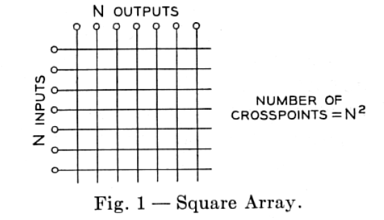
The simplest concept of a switch fabric is that known as a crossbar and is shown schematically in Figure 3. Here we have N inputs that could be connected to any one of N outputs. For now we can just think of simple port switching but the results and concepts apply to other forms of switching. In a crossbar fabric, to make a "connection" between an input port and and an output port requires the use of "cross point" element (some type of mechanical, electrical, or optical device). When a particular "cross point" element has been enabled we say a "cross connect" has been made.
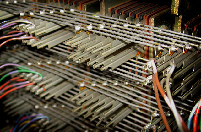
The name "crossbar" stems from the original mechanical electrical switches used in the telephone system where actual conducting "bars" where used to make connections semi-automatically. See Figure 4.
For automating our optical patch panel we need a mechanism to automate the "cross connects", i.e, to mechanize the cross points.
- How many cross points do we need for an N x N switch? An M x N switch?
- In the old mechanical switches and in current optical technology cross points can comprise the bulk of the switch cost and limits switch size.
- In electrical switches IC pin limits, fan out, delay, and signal degradation are important to.
- A big issue as the phone system got bigger was to reduce switch cost which implied trying to reduce number of cross points in a switch of a given size.
Multi-Stage Switch Architectures
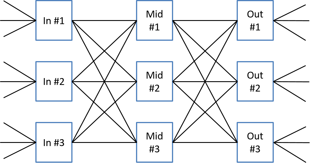
One approach that is both practical and can be effective is to build a large switch fabric out of a network of smaller sized switch fabrics. However arbitrary arrangements of elements may fail to yield any advantage as the following example shows.
Example: a 9 x 9 switch created with 3 x 3 elements
Consider my attempt shown in Figure 5 to create a 9x9 switch from 3x3 switching elements. As we can see I built a 9x9 switch out of 3x3 elements. So I managed to create a big switch from smaller packages. Did I reduce the number of cross points needed? A 9x9 switch needs 81 cross points, a 3x3 switch needs only 9 cross points, but I used nine 3x3 switches so ended up using 81 cross points again. Hence my design has no advantage with respect to cross points. Very disappointing so far, but it gets worse.
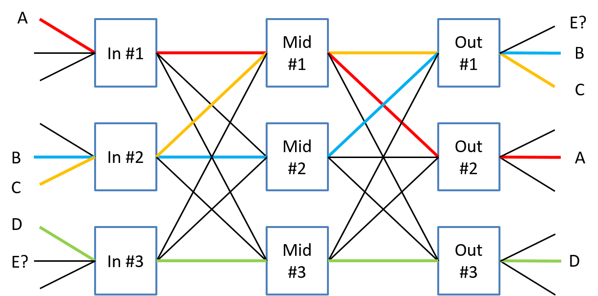
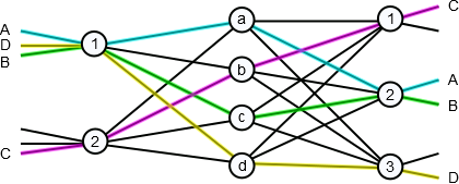
Now let's try to route connections across this multi-stage switch fabric. We denote a particular connection between an input port and an output port by a capital letter such as A, B, C, etc... We will place this letter alongside the respective input and output port to be connected as shown in the figure below. To make use of a multi-stage fabric we need to find a path across the fabric whose links have not been used by another connection. Remember we are thinking in terms of port switching, also known as space switching, right now and each connection between needs its own path and cannot share a path with any other connection.
In Figure 6 we give unique colors to the paths taken by connections so we can easily tell them apart (this has nothing to do with wavelength switching right now!). The figure shows sucessful paths for the connections A through D, but for connection E no path can be found that allows us to connect input switch #3 with output switch #1. Hence we see that connection E is blocked. Can we remedy this situation? If you look at connection D you'll see that three different paths are viable (through any of the middle switches). If connection D was re-routed through middle switch #2 rather than #3 then connection E could be accomodated through middle switch #3 to reach output switch #1.
As we have just seen an arbitrary attempt to design a multi-stage switch fabric resulted in no cost benefit (in terms of number of cross points) and performance issues (internal switch blocking). Some of the issues faced when developing a multi-stage switching network include:
-
The complexity of interconnection of the switching elements
-
The complexity of determining a path across this “mini-network”
-
Difficulty in figuring out if we can satisfy multiple connection requests simultaneously or incrementally.
Many different many multi-stage switch fabric architectures have been proposed over the years we will discuss one of the oldest and most sucessful. Variants of the design we will study have been and are used in TDM switches, optical switches and in the design of some of the highest performance datacenter networks yet built.
Three Stage Clos Networks
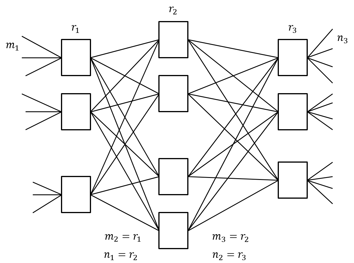
General Multi-Stage Clos Network: An interconnection network of smaller sized switches with a very simple and specific structure, Figure 7:
-
Each switch in each stage is the same size in terms of number of inputs and outputs
-
Each switch connects to one and only one switch in the next stage
-
At stage k we have $r_k$ crossbar switches, each with $m_k$ inputs, and $n_k$ outputs.
-
For a three stage Close network there are only 5 free parameters $m_1$, $n_3$, $r_1$, $r_2$, and $r_3$.
Strictly Non-blocking Clos Networks
Before we worry about cost optimization of our multi-stage fabric we first want to make sure that we can make connections across the fabric. This leads us to the following:
Definition (strict-sense non-blocking): A switching network is strict sense non-blocking if a path can be set up between any idle transmitter and any idle receiver without disturbing any paths previously setup.
Due to the relatively simple structure of a 3-stage Clos network we will be able to determine a simple criteria for strict sense non-blocking via some "creative bookkeeping".
Bookkeeping Connection Routing with Paull's Matrix [Paull1962]
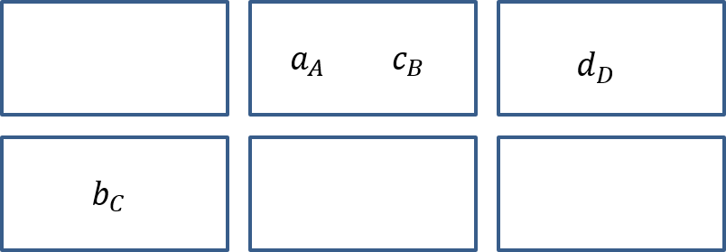
Consider the 3-stage Clos network shown in Figure 8 with $m_1 = 3$, $r_1 = 2$, $r_2 = 4$, $r_3 = 3$, and $n_3 = 2$. In general we will use numbers to denote the first (input) and third (output) stage switches and lowercase letters to denote the second (middle) stage switches.
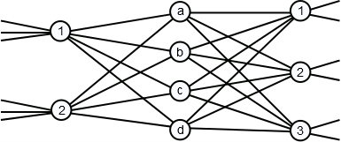
Now consider the four connections set up across our example switch fabric denoted with capital letters: A, B, C, D (in that order). See Figure 9.
- What would a complete specification of the path taken by connections A-D look like?
- What is the simplest way we can denote the paths taken by A-D?
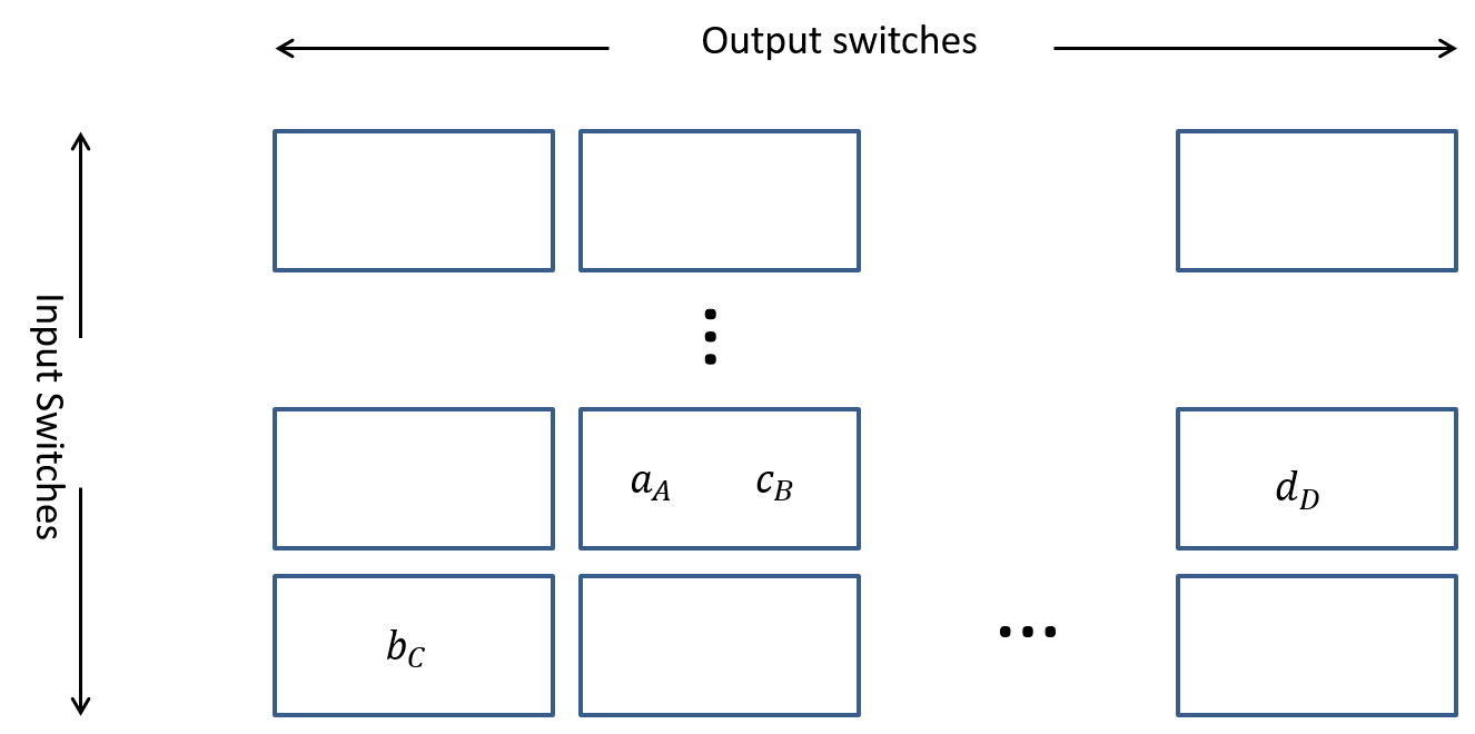
A connection a 3-stage Clos network is uniquely identified by its input switch, output switch, and middle switch identifiers. This is due to there being only one connection between each switch in a stage and a switch in the subsequent stage. One way to represent this in a form amenable to proving theorems or establishing algorithms is via Paull's matrix [Paull1962]. This "matrix" will have $r_1$ rows (one for each input switch) and $r_3$ columns (one for each output switch). We then put a letter representing the middle switch used for each connection in the row/column corresponding to the input and output switches. Note that we can have more than one letter per matrix entry. For our four connections above this would lead to the following matrix:
We show a general diagram of Paull's matrix in Figure 11 and note the following important properties of this "matrix":
- At most $m_1$ entries per row. Reason: A row represents a particular input switch and these switches have only $m_1$ input ports. Hence we can never get more than $m_1$ entries into a row.
- At most $n_3$ entries per column. Reason: A column represents a particular output switch and these switches have only $n_3$ output ports. Hence we can never get more than $n_3$ entries into a column.
- All entries in any row or column must be unique with a maximum of $r_2$ total entries in any row or column. Reasoning: The uniqueness of entries in a row (meaning the letters used to denote the middle switches) is due to the limit of each input switch connecting to one and only one middle switch. The uniqueness of entries in a column stems from each middle switch connecting to one and only one output switch. The maximum number of distinct entries in a row or column is limited by the number of middle switches $r_2$.
Now we are in a position to establish Clos's Theorem on when a 3-stage Clos network is strict sense non-blocking.
Worst case situation:
- An input switch X has $m_1-1$ of its inputs used
- An output switch Y has $n_3-1$ of its outputs used
- We want to connect the last unused input input $m_1$ of X to the last unused output $n_3$ of Y.
Paull’s matrix bookkeeping implications:
- For the row corresponding to input switch X we will have used $m_1-1$ unique symbols. Remember symbols (lowercase letters) identify the middle switch used in the connection.
- For the column Y will have used $n_3-1$ unique symbols.
- In the worst case scase all of the symbols used are unique so we have used a total of $m_1 + n_3 -2$ symbols (middle switches) and to complete this last connection we need one more so our strict sense non-blocking criteria is that the number of middle switches $r_2 \geq m_1+n_3-1$.
Theorem (Clos) A three stage Clos network is strict sense non-blocking if $r_2 \geq m_1+n_3-1$.
Better Cross Point Scaling with a Clos Network
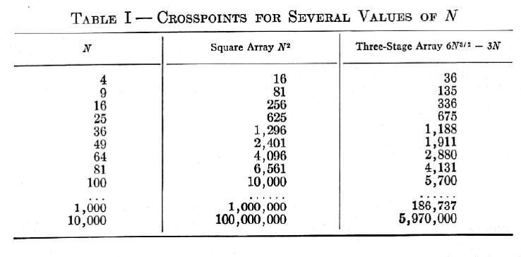
Now that we've seen how to insure that a 3-stage Clos network will be strict sense non-blocking let's see if we can do better on the cross point count. In Figure 12 we show an example from Clos's original 1953 paper [Clos1953]. In this example the goal was to create a switch with $N=36$ input and output ports. The parameters $m_1 = 6$ and $n_3 = 6$ were chosen which implied that $r_1 = 6$ and $r_3 = 6$ to satisfy the sizing and that $r_2 = 11$ to insure strict sense non-blocking.
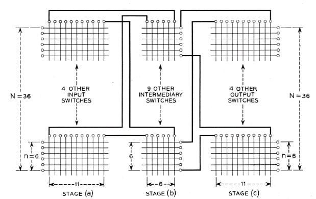
The input switches have size 6x11 and there are be 6 of them leading to 396 cross points. The middle switches have size 6x6 and there are be 11 of them leading to 396 additional cross points. Finally the output switches have size 11x6 and there are six of them leading to another 396 cross points, giving us a total of 1188 cross points. For a 36x36 crossbar we would need 1296 cross points so we have saved 108 cross points! Okay, that doesn't sound so impressive but let's see how this scales up...
To scale his fabrics up Clos' made the following assumptions:
- Symmetrical network (same number of inputs as outputs = N)
- Number of network inputs is a perfect square $N = n^2$
- The 3-stage network parameters are:
- $m_1 = n$ and $r_1 = n$ the number of inputs on the first stage switches and the number of first stage switches.
- $n_3 = n$ and $r_3 = n$ the number of outputs on the third stage switches and the number of third stage switches.
- Clos’ Theorem for strict sense non-blocking then requires $r_2 = 2n-1$
Now let's us do the bookkeeping on the number of crosspoints:
- Input Switches (number n)
- Size = $n \times (2n-1)$
- Input switches total cross points = $2n^3 - n^2$
- Middle Switches (number $2n-1$)
- Size = $n \times n$
- Middle switches total cross points = $2n^3 - n^2$
- Output Switches (number n)
- Size = $(2n-1) \times n$
- Input switches total cross points = $2n^3 - n^2$
- Grand total number of cross points
- $6n^3 - 3n^2$ but since $N = n^2$ this gives $$6N^{3/2} - 3N$$.
Hence instead of $O(N^2)$ a 3-stage Clos network has $O(N^{1.5})$ growth! In Figure 13 we show the comparison table from Clos' original paper which illustrates the crosspoint savings as N grows larger.
Pin Count and Power Limitations
As we move forward from the 1950's to the 2000's and beyond Clos networks are still useful and important but other optimization criteria besides the number of cross points may take precedence. In Clos's table we saw that a crossbar based switch with 10,000 inputs and outputs would require 100 million cross points and a 3-stage Clos less than 6 million. With electrical technology one can implement a cross point with a single CMOS transistor (ignoring fanout and fan-in issues). A relatively modern smart phone circa 2015 will contain one to two billion transistors. Hence today we have tons of cross points to spare. However, power and heat disipation is still an issue and by reducing the number of cross points we significantly save on power.
There is a more subtle issue that gives rise to an interest in Clos networks in large switch implementations and that is pin count limitations associated with integrated circuit packaging. While the amount of logic that one can put on an integrated circuit has increased exponentially over the years the increase in the number of input and output pins (electrical connections) one can attach to an integrated circuit has not kept pace. Two of the densest forms of packaging are ball grid arrays and flip chip ball grid arrays. These dense packaging technologies have pin count limits in the range of 3000 pins. If we wish to use a single integrated circuit as a switching element in a multi-stage fabric we must keep these limits in mind.
Rearrangeably Non-Blocking Clos Networks
In Clos's symmetric 3-stage fabric $m_1 = n$, $n_3 = n$, and $r_2 = 2n-1$ for strict sense non-blocking. This led to switches of sizes $n \times (2n-1)$, $n \times n$, and $(2n-1) \times n$ for stages one through three respectively. We see that the strict sense non-blocking criteria of $r_2 = 2n-1$ is pushing up the first and third stage switch sizes and hence their pin counts. Is there any less rigorous requirement than that of strict sense non-blocking? In particular what if we are allowed to rearrange the paths taken by existing connections through the fabric to accommodate a connection? It turns out there is a fundamental result along these lines.
Theorem (Slepian-Duguid Theorem) [Hui1990]
A three stage Clos network is rearrangeably non-blocking if and only if $r_2 \geq max(m_1, n_3)$.
This result, if we can tolerate the rearrangements, allows for a pin count reduction of about $1/3$ for the first and third stage switches. Let's see an example of how this works. In Figure 14 below we show a 3-stage Clos network built from 4x4 switches $m_1=4$, $n_3 = 4$, since $r_2 = 4$ the criteria for strict sense non-block is not met and we see that there is no open path to make the connection J which wants to go from input switch 3 to output switch number 3.
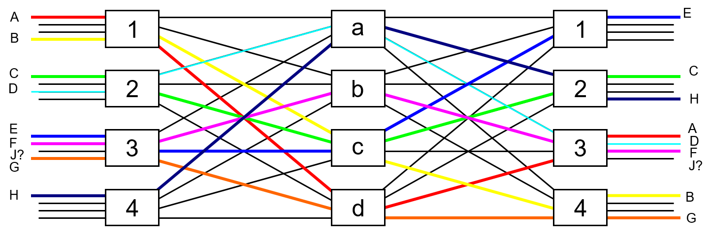
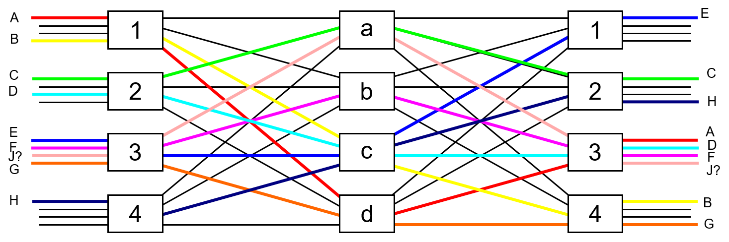
In Figure 15 we show that by rearranging the paths of connections C, D, and H, then a path through the fabric could be found for connection J.
Figuring out which connections to rearrange and where to move them is non-trivial, one algorithm for doing this is given below. Note that these techniques (and more advanced) are actually used in real switches. The author of these notes led a software development team on a very large electro-optical switch that featured a 3-stage rearrangeably non-blocking Clos fabric and that saw worldwide deployment in carrier optical backbone networks.
Algorithm to establish a connection between input switch SI and output switch SO, given Paull’s matrix of existing connections for a Clos network satisfying the above criteria.
Step 1 (no-rearrangement, connect). Check if there exists a middle switch “symbol” (e.g., we’ve been using lower case letters) which is not found in both row SI and column SO. If so then you can use the middle switch represented by this symbol to make the connection. Otherwise go to step 2.
Step 2 (discovering a rearrangement chain).
(a) Find a symbol x in row SI which is not found in column SO and find a y in column SO not found in row SI. (Note that such symbols must exist). Remember these x and y symbols and where you found them.
(b) Check the row where you found the y above to see if an x symbol is present if not proceed to step three, otherwise remember this x and go to step (c).
(c) Check the column that the x appeared in step (b) to see if a y appears if not go to step 3, otherwise remember this y and go to step (b).
Step 3 (rearrange and connect) Put a y in (SI, SO) of Paull’s matrix and swap all x with y in the “chain” from step 2. (Note that the first x is not part of the chain).
Clos Networks and Large Data Centers
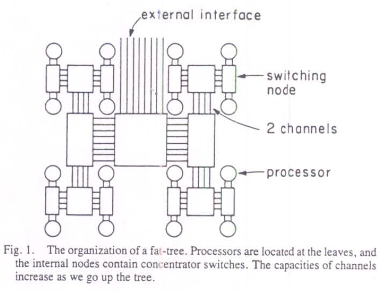
In 1985 with the goal of designing a better communications network within a highly parallel supercomputer a network architecture called a fat tree was published [Leiserson1985]. A key feature, shown in Figure 16, is that the network is arranged in a tree structure with the processors as the leaf nodes and as one moves up the tree more bandwidth is made available between the switches. This led to the name fat tree for such a structure.
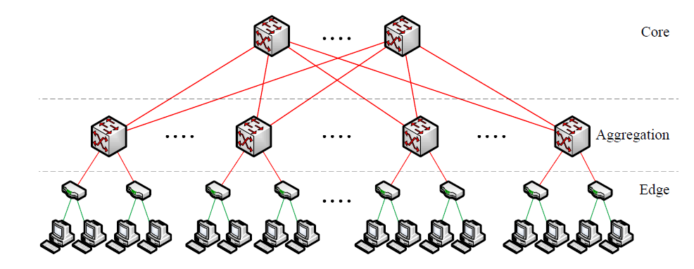
In 2008 citing issues with traditional data center network topologies, as shown in Figure 17, for modern compute applications (Map/Reduce, etc...) Al-Fares et. al. [Al-Fares2008] proposed a new data center topology based on a Clos topology with faster switch to switch links than switch to host links. Note that in the traditional data center topology shown below the host to switch links were 1Gbps and the switch to switch links were 10Gbps hence the "fat tree" nature wasn't the new feature of their proposal.
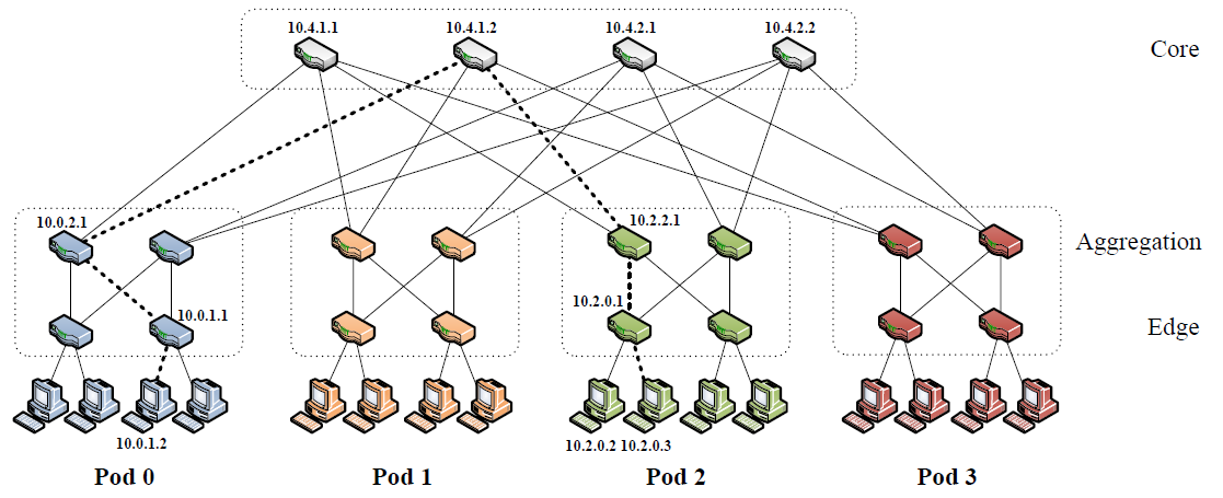
What was new in the Al-Fares network, shown in Figure 18, was the use of a 3-stage Clos topology between their aggregation switches and their core switches. This may not initially look like the 3-stage Clos network that we studied, but this is only due to the links in the diagram being bidirectional as contrasted our use of unidirectional links when we previously drew our Clos networks. Note also we are using the term switch in its generic sense, in the Al-Fares network Layer 3 switching (IP routing) was used.
Key points made by Al-Fares et. al. [Al-Fares2008] include the need for Equal Cost Multi-Path (ECMP) to distribute IP traffic over multiple paths, and the fact that the Clos network built in this way will be rearrangeably non-blocking.
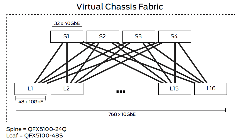
As of 2014 we were saw Clos topologies for data centers showing up in a Juniper white paper, see Figure 19. Some nicer terminology is coming into use with the "edge" switches called leaf switches and the "core" switches called spine switches. At the end of 2014 one very large data center, Facebook, announced that it was using 5-stage Clos networks with commodity switch fabrics Facebook's data center fabric. Note that this post includes a nice video with animations. For a very complete review of Clos for data centers featuring a control plane based on BGP, see BGP large DC.
Finer Granularity Switches
We’ve looked at how to create very large capacity switches via cross points, crossbars, and multi-stage switch fabrics. There is one problem with the switches we've designed so far: they switch the entire "content" from an input port to a selected output port. This is extremely coarse granularity switching and while useful in the proper context we will need other techniques to acheive finer granularity. We also note that the coarse granularity "port to port" switching we have been discussing is also called space switching.
Now we will look at a general techniques useful for finer granularity switching. All our techniques will be based on electronic rather than optical technology.
Slowing Things Down for Electronic Processing
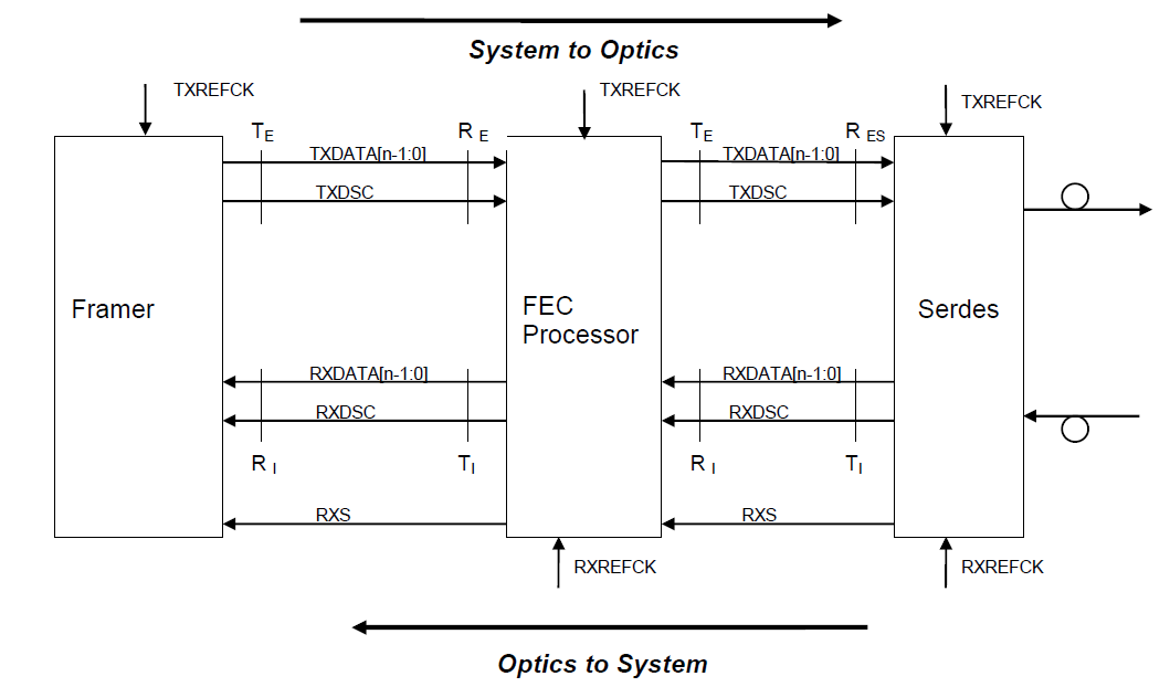
In Figure 20 below we show standardized interfaces,OIF-SFI-S-01, between (right to left) optical transmitter and receiver, a Serdes (serializer-deserializer), FEC (forward error correction) processor, and a TDM (G.709, SDH, SONET) or link layer framer. In the specification the number of lanes n ranges from 4 to 20. This specification is aimed at optical interfaces running at between 80-160Gbps. Note that since the signals have yet to be processed by the framer no byte boundaries have been determined.
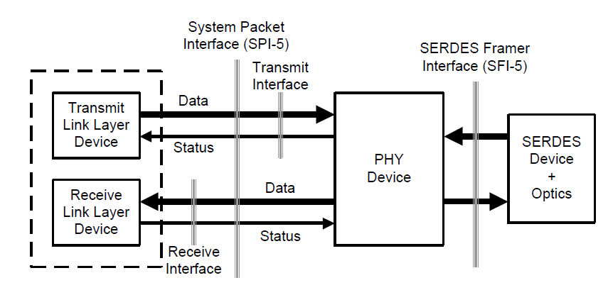
In the Figure 21 we show an early 2000's system packet interface, OIF-SPI5-01, which featured 16 bit wide data interfaces for transmit and receiving from the somewhat misnamed PHY Device (actually a TDM framer). This was aimed at optical interfaces running in the 40Gbps range.
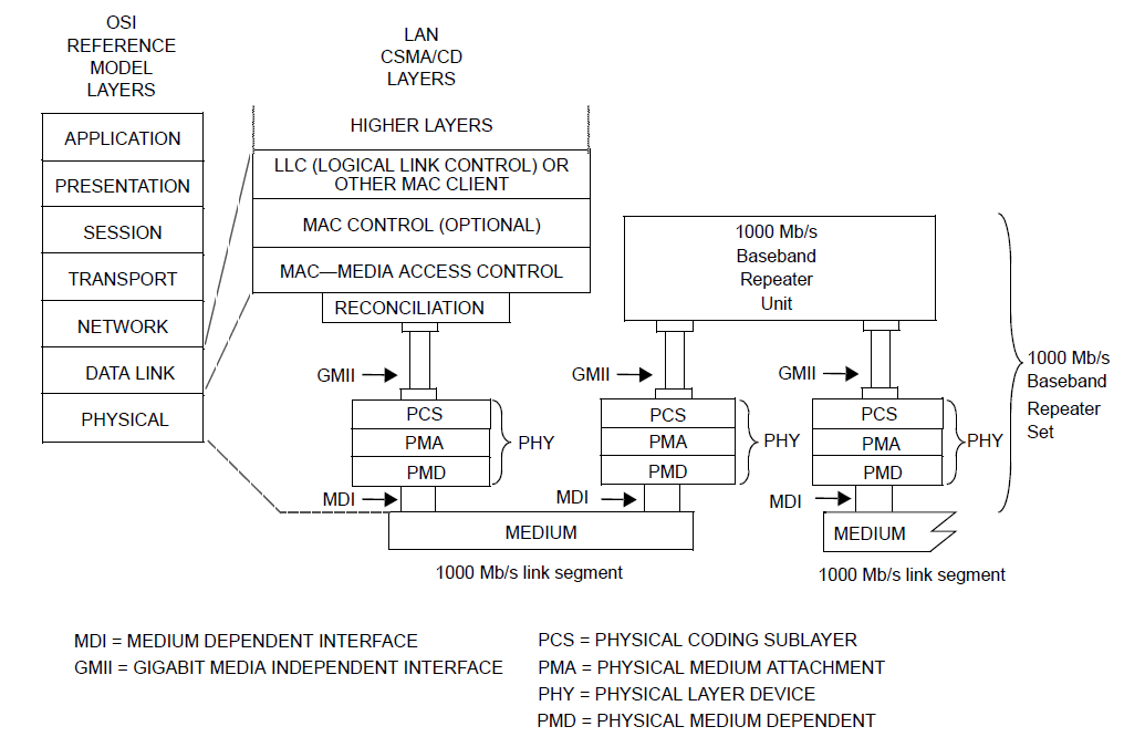
Such conversion from serial to parallel isn't just used in optical situations. In Figure 22 we shown a layer diagram for Gigabit Ethernet from the IEEE 802.3-2012 section 3, chapter 34. We see in this diagram above the various physical sublayers (PMD, PMA, PCS) there is a gigabit media independent interface (GMII).
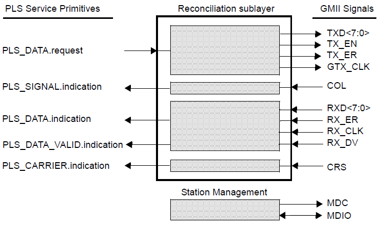
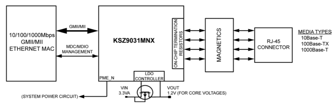
The GMII interface, Figure 23, features 8 bit wide transmit and receive interfaces. In Figure 24 an example use of the GMII interface in shown, from a micrel Gigabit Ethernet Transceiver datasheet.
Note that while wider interfaces allow the use of lower speed signals they also use more integrated circuit pins. Hence much of the "widening" now a days occurs internal to a chip.
TDM switching via Time Slot Interchange
As our first example of a fine grainularity switch let's build an switch that works with time division multiplexed signals and switches at the level of a DS0 (64kbps). In Figure 25 we show a block diagram of our switch that takes in 10 bi-directional T1 lines and can switch any (input port, time slot) to any (output port, time slot).
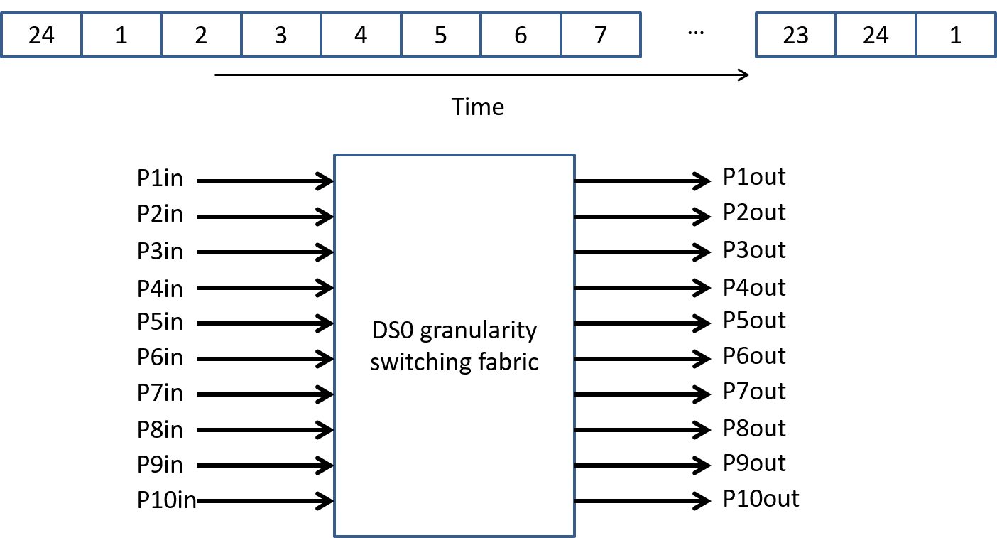
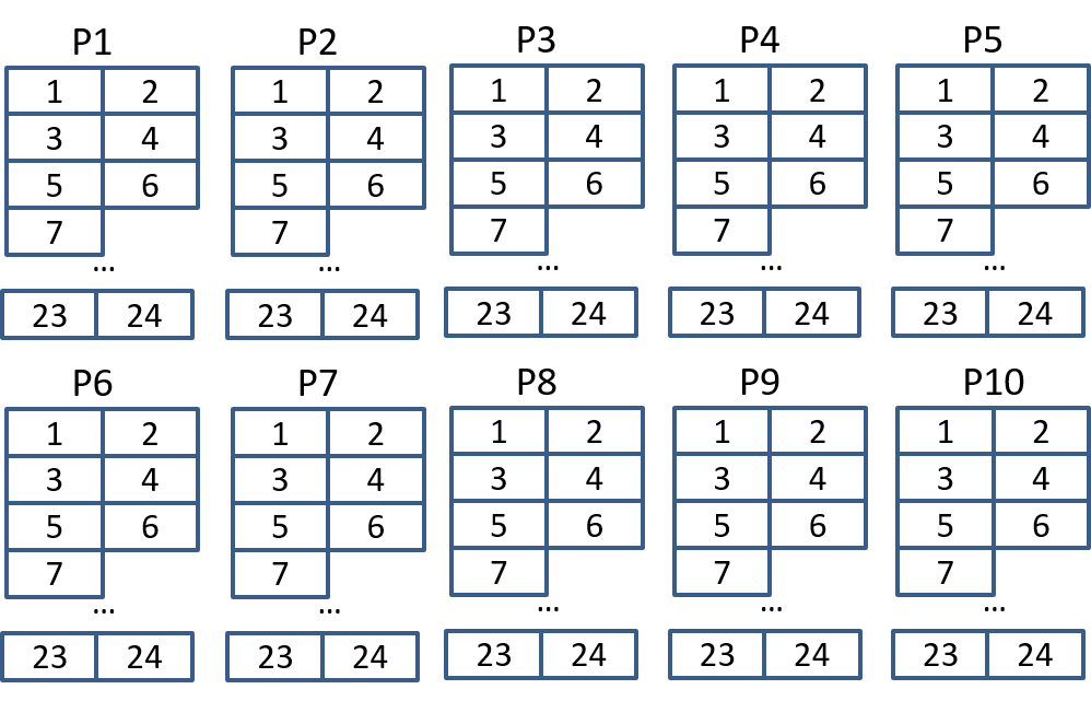
Basic idea: write all the incoming data into bytes of memory associated with the particular port and time slot. Read data back out to proper output port and time slot. A "memory map" for this is shown in Figure 26. Note that we are essentially switching in time (due to time slot interchange) and in space (across ports).
How much memory will we need? Let’s assume that everything is synchronous (not really true but framers have small FIFOs to take up the slack), and that we can’t read and write the same memory location at the same time. In this case we’ll use two memory locations per time slot and alternate reading and writing from those locations. So given 10 T1 lines, 24 byte time slots per T1, and 2 memory spaces per timeslot = 480 bytes of memory. That is an insignificant amount of memory even for a micro-controller.
How fast does the memory need to be able to operate? Assume byte wide memory and that read and write operations must be separate. For a T1 we have 24 bytes every 125us, 10 T1s => 240 bytes every 125us, read/write separate ==> 480 bytes every 125us ==> 0.261us per byte.
How does this compare with modern SRAM access times? Inexpensive small RAMs have access times between 15-150ns hence are twice to 10 times as fast as this.
Or we can think of this as (10 T1s)*(1.5Mbps per T1)*(2 separate read/write) = 30Mbps transfer rate memory.
Packet Switching via a Shared Memory Fabric
Now lets design a packet switch via the shared memory approach. How about 8 ports of 1Gbit Ethernet. Assume that we might have to buffer up to 100 Ethernet MTUs per output port.
How much memory space would we need? (8 ports)*(1500 bytes/MTU)*(100 MTUs) = 1.2e6 bytes. Much bigger (4 orders of magnitude) than the TDM case.
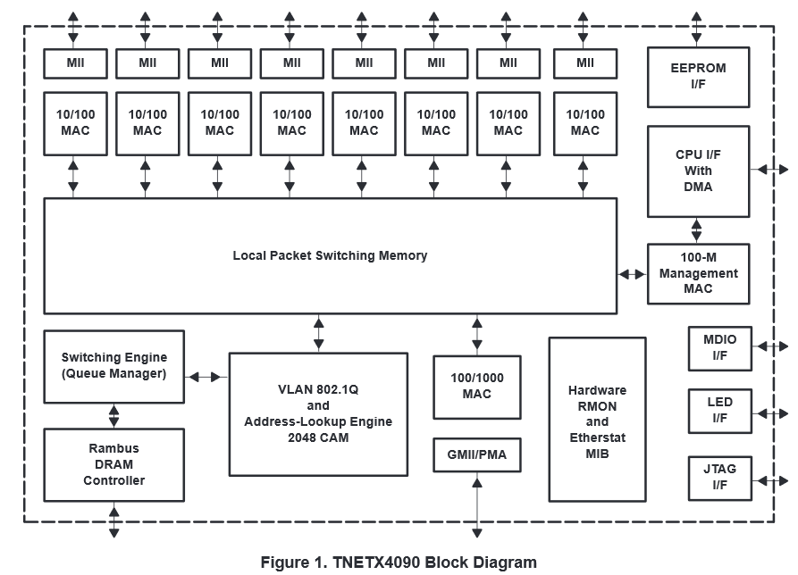
How fast would the memory need to operate? Raw: 16Gbits/sec for separate read and write. Where can we get this type of memory speed and size? Or should we give up? First let's check the speeds of common DRAM used in computers at Wikipedia (DRAM). Looking at this table we note that 133MHz DDR comes in around 17Gbps. But wait a second isn't SRAM supposed to be faster than DRAM? Where did this extra speed come from? DDR SDRAM uses a bus that is 64 bits wide. Would someone actually make a switch this way? Yes and No. In Figure 27 we show a block diagram for an Ethernet switching chip circa 1999 which features access to external DRAM via a "Rambus DRAM controller".
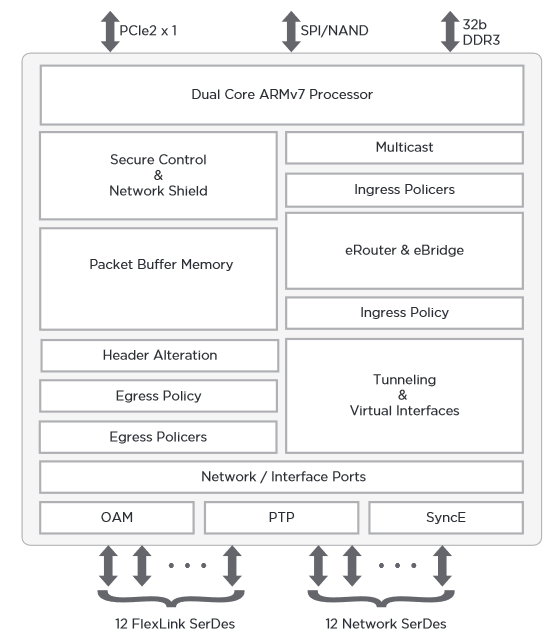
With the every increasing density of memory and "system on a chip" (SoC) technology that allows integration of relatively large amounts of memory, packet buffers are frequently kept on chip as Figure 28 from a relatively recent Marvell product brief shows. This trend is seen with other manufacturers and discussed at length in a 2012 Broadcom white paper where they state: "Today, traditional fixed switch designs using distributed chipsets and external packet buffers have been largely replaced by highly integrated devices with on-chip buffering."
There are limits to the size of the memory that can be put on chips along with the switching functionality. Publically available information isn't readily available on how large these are on current chips however an estimate can be gotten by looking at trends in L3 caches in high performance processors where these can be 8MB or more (circa 2015). The other interesting trend noted in the L3 cache article is that in new multi-core processors the L3 cache is shared amongst multiple processors. The shared L3 cache scenario is very similar to a shared memory switch fabric and the crux of the previously noted Broadcom whitepaper was on shared memory management.
Input Packet Processing
After we've suceeded in getting our packet into our switch, we now need process it and send it out. What kind of processing might be required on a packet? Any of the actions that we learned about when we studied tunneling, VLANs, MPLS, and software defined networks (SDNs). Here's just a short sample of the packet processing that might be down on initial input:
- IP Processing
- Longest match address prefix lookup
- Increment TTL counter
- Modify type of service bits, and/or, congestion control bits
- Encapsulate/De-encapsulation tunneling protocols
- MPLS Processing
- FEC (Forwarding Equivalence Class) classification (edge Label Switch Routers)
- Label look up
- Label push and pop operations
- Ethernet
- Ethernet adddress look up
- VLAN tag addition or removal
- Modify QoS bits
- SDN (OpenFlow data plane processing)
- Priority based generalized packet header matching
- Generalized packet header processing
How much time do we get to do these and potentially other operations? To avoid our packet processing becoming a bottleneck (rather than the rate of the ingress or egress port) we need to complete our header processing by the time the entire packet is completely received. Note that except for potentially some checksums that are done over the entire packet (and are readily computable at line rate in hardware) the input processing (and most output processing) is only concerned with processing the header. Hence a larger total packet size gives us more time to process the header. Thus we see that smaller packets are more challenging for input processing than larger.
Example
What is the worst case header processing rate we would need to meet for the eight 1 Gbps port Ethernet switch we investigated in our shared memory packet switch design? Assume smallest Ethernet packet is 64 bytes long. The worst case total switch input rate is 8Gbits per second, so we would get a worst case input packet rate of 8Gbps/(64 bytes/Packet * 8 bits/byte) = 15.625 million packets/second. Or 64 nano seconds per packet worst case.
How could get more time to process our packets? One approach is partition the input processing amongst groups of links rather than processing all links with the same input processor. In the extreme we could dedicate an input processing unit to each link and in the example above this would give us 512 nano seconds to process the header. The downside of such an approach is that it requires us to duplicate the hardware required for input processing multiple times thereby driving up the cost of the hardware. To help switch buyers tell if their switch manufacturer has cut corners on input processing capabilities or in other areas, switching benchmarks (test proceedures) should be consulted. One useful LAN switching benchmark is RFC2889.
Lookups, Matches, and Such
What is the most computationally difficult operation that needs to be performed on packet ingress? In the bullet list of packet operations I purposely put the hardest first: IP — longest match prefix lookup; MPLS — FEC matching and label lookup; Ethernet — address lookup; SDN — prioritized general header matching. All these are variants of a search problem and hence as the number of entries in our table (IP prefixes, Ethernet addresses, MPLS labels, SDN matches) grows we may run out of time to complete our search. Or as is more commonly encountered to achieve the desired lookup speed specialized hardware is used that places fairly restricted limits on the table size. In the following we quickly look at two common hardware techniques used to perform the search operation needed for input packet processing.
TCAMs for General Matches
A key aspect of IP addresses is the hierarchical nature of their assignments to geographic regions, countries, ISPs and such. This allows IP addresses within a given domain to be summarized by only a portion of the full length of the address, known as a prefix. This greatly reduces the size of IP address tables in routers. Since different domains may be vastly different in size, the prefixes used in IP routing have variable size and this lead to IP's longest match rule. For software based routers concerned with performance, optimizing such matches led to very specialized search algorithms based on trees.
As networking speeds increased the longest match search was implemented in specialized hardware known as a content addressable memory (CAM). The name content addressable memory is a bit confusing but its really just a hardware lookup/search implementation. Such specialized memories are frequently used in the memory management units of almost all advanced processors and in that case are called translation lookaside buffers (TLB). For longest match searches or for general matching such as in MPLS FEC classification or SDN we need the ability to indicate "don't care" or "wild card" fields and the type of CAM that supports this is called a ternary CAMs (TCAM).
Now in addition to longest match IP address searches TCAMs play and important role in MPLS classification and OpenFlow. TCAMs may appears as separate integrated circuits or with system on a chip switch designs. Critical parameters include the bit width of the key (portion of packet header to search against), the size of the memory and the lookup speed.
Hardware Hash Tables
While very general and fast, TCAMs can be costly for the amount of table space they provide. For more specific types of look up other mechanisms have frequently been employed. If one considers destination based Ethernet forwarding the look ups are based on the entire 6 byte Ethernet address with no wildcard fields involved. Such a restrictive lookup (search) is amendable to fast hardware implemented hash tables. For an overview of how these can be implemented see this post on hardware hash table implementation issues.
For more on hash table and TCAM and their strengths and weakness see the following posts:
- Blog post on Hash Tables versus CAMs. Has good definitions of Hash tables, CAMs, and TCAMs.
- Blog post on ternary hashing, i.e., doing varible length matching with hash tables in hardware.
- Blog post on SDN TCAMs and hashes. The difficulty of general SDN matches for either TCAMs or hashes.
Multiple Lookup Tables
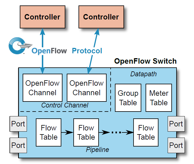
It is the limits on TCAM size and width, and better alternatives for more specialized searches that led to the multiple table model that we saw in OpenFlow 1.1 and later (Figure 29).
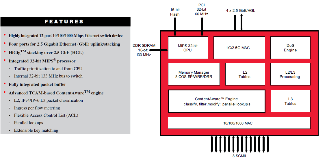
We also see this in system on a chip switch implementations as shown in Figure 30 which specifically mentions a TCAM based solution, but shows space for separate L2 (Ethernet) and L3 (IP) tables.
References
Note that BSTJ articles are available free from http://www3.alcatel-lucent.com/bstj/
- [Paull1962] M. C. Paull, “Reswitching of Connection Networks”, Bell System Technical Journal, vol 41, no 3, bll 833–855, 1962.
- [Clos1953] C. Clos, “A Study of Non-Blocking Switching Networks”, Bell System Technical Journal, The, vol 32, no 2, bll 406–424, Mrt 1953.
- [Hui1990] J. Y. Hui, Switching and Traffic Theory for Integrated Broadband Networks. Norwell, MA, USA: Kluwer Academic Publishers, 1990.
- [Leiserson1985] C. E. Leiserson, “Fat-Trees: Universal Networks for Hardware-Efficient Supercomputing”, IEEE Trans. Comput., vol 34, no 10, bll 892–901, 1985.
- [Al-Fares2008] M. Al-Fares, A. Loukissas, en A. Vahdat, “A Scalable, Commodity Data Center Network Architecture”, in Proceedings of the ACM SIGCOMM 2008 Conference on Data Communication, 2008, bll 63–74.